
{{product.productLabel}} {{product.model}}
{{#if product.featureValues}}{{product.productPrice.formattedPrice}} {{#if product.productPrice.priceType === "PRICE_RANGE" }} - {{product.productPrice.formattedPriceMax}} {{/if}}
{{#each product.specData:i}}
{{name}}: {{value}}
{{#i!=(product.specData.length-1)}}
{{/end}}
{{/each}}
{{{product.idpText}}}
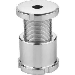
... 1.7225. Stainless steel 1.4305.Version:Seel version trivalent blue passivated. Stainless steel version bright.Note:Levelling sets are used for mounting, levelling and aligning motors, aggregates, drive units and assembly ...

What is Die Ace ? Die Ace is a material developed for draw dies for press stamping. It is a highly hardened special copper alloy casting. Die Ace can smoothly function ...
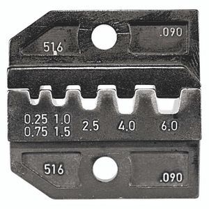
Weight - 40 g Dimension - 32 mm Number of crimping positions - 5 Capacity - 0.25 – 0.75 mm² / 1.0 – 1.5 mm² / 2.5 mm² / 4.0 mm² / 6.0 mm² Connector - Ferrules for PEW 12 - ✔ for E-PEW 12 - ✔ for CM 25-1 - ✔ for CM 25-5 ...

Weight - 40 g Dimension - 32 mm Number of crimping positions - 3 Capacity - 25.0 mm² / 16.0 mm² / 10.0 mm² Connector - Ferrules for PEW 12 - ✔ for E-PEW 12 - ✔ for CM 25-1 - ✔ for CM 25-5 - ✔ for CM 25-6 - ✔
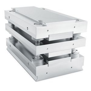
We offer you our SB stamping and forming die sets for the 200 kN, 300 kN and 400 kN Bihler presses. The die sets are available from stock in lengths up to 596 mm and ...

... includes die sets as per DIN / ISO and company standards made of steel, cast or aluminium with slide or ball guide. We also distribute small presses, precision tool assemblies and quick ...

Combi-die sets with down-mounted columns Combi-die sets with aerial-mounted columns Die set plates Guide pillars Guide pillars with ...
STRACK NORMALIEN

... The standard 5-part pellet dies consist of a base, a body, 2 pressing pellets between which the sample is pressed as well as a plunger. In addition, 2 O-rings are used to complete the die and enable superior ...

Die Sets (SFG) are manufactured product-specifically and offer the advantage of setting a large number of clinching joints in just one press stroke. Bending or punching processes can also be integrated ...
REF. 5630 REF. 5680 REF. 5683 REF. 5670 REF. 5660 DEMOUNTABLE BLOCK

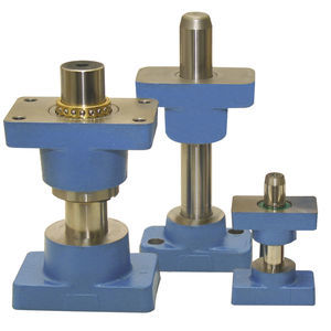
ST1001 Die set upper part without thread, with sliding guide, bronze coating Referring to DIN 9812 Material Grey cast irons EN-GJL-250 Upper plate without thread Type ...

For over 40 years, die makers have been building their stamping dies with die sets from Anchor Lamina. Anchor die sets are manufactured ...
Please specify:
Help us improve:
remaining