
{{product.productLabel}} {{product.model}}
{{#if product.featureValues}}{{product.productPrice.formattedPrice}} {{#if product.productPrice.priceType === "PRICE_RANGE" }} - {{product.productPrice.formattedPriceMax}} {{/if}}
{{#each product.specData:i}}
{{name}}: {{value}}
{{#i!=(product.specData.length-1)}}
{{/end}}
{{/each}}
{{{product.idpText}}}

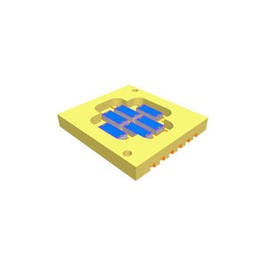
Surface mountable 16-element array The S15158 is a 16-element Si PIN photodiode array in surface mountable chip carrier package. It can be mounted using solder reflow and used in a wide ...

4X200Gbps 500μm Die Pitch 1X4Array Bottom-illuminated PIN PD Chip This 4X112GBaud Array 800Gbps photodiode chip, which is bottom-illuminated and mesa structure high data rate PIN photodiode ...
PHOGRAIN TECHNOLOGY(SHENZHEN) CO., LTD.

Description The 8X56Gbaud (8X112Gbps PAM4) array light detector chip is a high-speed digital PIN light detector chip with a top entry light and a mesa structure, and the photosensitive zone size is Φ20μm. Characterized ...
PHOGRAIN TECHNOLOGY(SHENZHEN) CO., LTD.
Description This high data rate 4X28Gbps NRZ/4X56Gbps PAM-4 photodiode chip is GaAs top- illuminated 1x4 Array PIN structure. Features are high responsibility, low capacitance and low dark current, ...
PHOGRAIN TECHNOLOGY(SHENZHEN) CO., LTD.
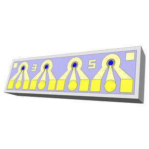
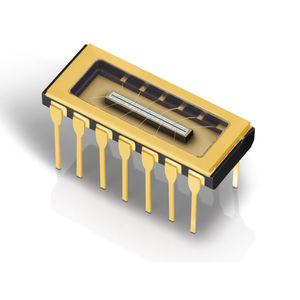
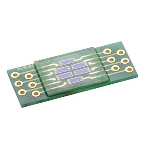
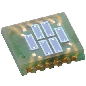
OID7 6 p/n photodiode array chip General Description Optical device consisting of a 6 chip silicon P/N photodiode array with high uniformity for the output signals. ...
... elements. The arrays can be configured to fit the customer’s requirement in terms of the number and size of the array elements. 8-, 12- or 16-element arrays in a 14-pin DIL package are ...
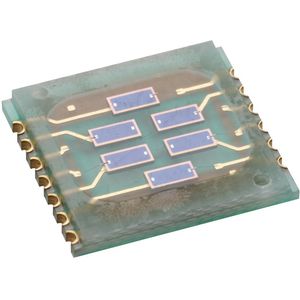
... consists of 6-chip photodiodes produced in planar technology. The photodiodes are passivated with silicon-nitride which acts as an antireflective layer. They are then bonded to the PCB and protected with ...
... consists of 6-chip photodiodes produced in planar technology. The photodiodes are passivated with silicon-nitride which acts as an antireflective layer. They are then bonded to the PCB and protected with ...
... consists of 6-chip photodiodes produced in planar technology. The photodiodes are passivated with silicon-nitride which acts as an antireflective layer. They are then bonded to the PCB and protected with ...
... ILLUMINATED PHOTODIODE ARRAYS CUSTOM PRODUCTS Share on FacebookTweet about this on TwitterShare on LinkedInEmail this to someone Backside illuminated (BSI) photodiode technology ...
Detection Technology

The photodiode array is composed of several photodiodes arranged in a line or a matrix, forming a single component.
ApplicationsThe photodiode array has many applications. It is used for laser beam alignment, color measurement and in spectrophotometry.
TechnologiesSometimes the array signal is read by a multiplexer using CMOS technology. This simplifies both the design and the output circuit.
How to chooseThe selection of a photodiode array depends on the intended application. This will dictate the choice between a linear or matrix model. Wavelength detection range is another important factor.
- Sensitivity
- Price
- Broad detection range
- Dark current
Please specify:
Help us improve:
remaining