

{{product.productLabel}} {{product.model}}
{{#if product.featureValues}}{{product.productPrice.formattedPrice}} {{#if product.productPrice.priceType === "PRICE_RANGE" }} - {{product.productPrice.formattedPriceMax}} {{/if}}
{{#each product.specData:i}}
{{name}}: {{value}}
{{#i!=(product.specData.length-1)}}
{{/end}}
{{/each}}
{{{product.idpText}}}

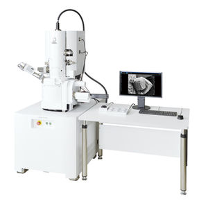
Magnification: 3,000,000 unit
Resolution: 0.8, 0.4, 1.2 nm
The Cold Field Emission source is ideal for high-resolution imaging with a small source size and energy spread. Innovative CFE Gun technology contributes the ultimate FE-SEM with superior beam brightness and stability, affording high-resolution ...

Magnification: 5 unit - 800,000 unit
Resolution: 15, 4, 3 nm
Performance & Power in a Flexible Platform Hitachi High-Tech's scanning electron microscopes SU3800/SU3900 deliver both operability and expandability. The operator can automate many operations and efficiently utilize ...

Magnification: 20 unit - 8,000,000 unit
Resolution: 0.08, 0.1 nm
... electron gun (Cold FEG) • Ultra-stable column and power supplies for enhanced instrument performance • Simultaneous Cs-corrected SEM & STEM imaging capability with atomic resolution • New high-stability side-entry ...

Resolution: 1 µm
The MX63 and MX63L microscope systems are optimized for high-quality inspections of wafers as large as 300 mm, flat panel displays, circuit boards, and other large samples. Their modular design enables you to choose the ...
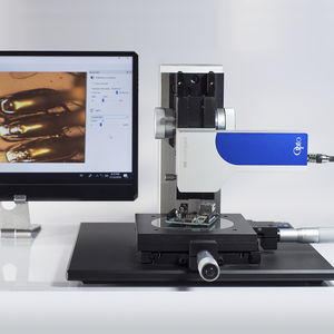
The new "Machine Vision Microscope" (MVM) is a purely digital microscope with all the features that make a microscope. It has an apochromatically highly corrected microscope ...
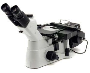
... analyzes. Entry-level inverted microscope for general purpose applications for hardness testing. Industrial and materials science inverted microscope especially designed for opaque specimens (including ...

ZTX-S series zoom microscope adopts optical imaging system,with high resolution,fine definition and strong sense of three-dimensional,easy operation.The microscope is Widely used in semiconductor ...
Magnification: 10 unit - 2,740,000 unit
Resolution: 0.9, 1.3 nm
... integrates SEM imaging and EDS analysis. This powerful function provides next-generation operability and high resolution images obtained with FE-SEM. New "Zeromag" function "Zeromag", incorporated for seamless transition ...

Resolution: 0 nm - 100 nm
Extreme research systems for nanomechanics, nanoelectrical and nanoelectrochemistry Bruker’s Dimension XR scanning probe microscope (SPM) systems incorporate decades of research and technological innovation. With routine ...

Weight: 17 kg
Length: 490 mm
Width: 251 mm
The ECLIPSE LV100N POL and Ci-POL series of polarising microscopes is used to study the birefringent properties of anisotropic specimens by observing image contrast and colour changes. Nikon offers systems for both quantitative ...
Nikon Metrology
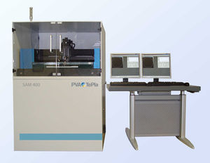
... new rf and transducer technologies of up to 400 MHz, controlled through a user friendly graphical interface. Built to semiconductor industry standards around a core platform that utilizes the latest production and research ...
PVA TePla Analytical Systems GmbH
Please specify:
Help us improve:
remaining