
{{product.productLabel}} {{product.model}}
{{#if product.featureValues}}{{product.productPrice.formattedPrice}} {{#if product.productPrice.priceType === "PRICE_RANGE" }} - {{product.productPrice.formattedPriceMax}} {{/if}}
{{#each product.specData:i}}
{{name}}: {{value}}
{{#i!=(product.specData.length-1)}}
{{/end}}
{{/each}}
{{{product.idpText}}}

DC voltage: 9.2 V - 748.65 V
Reverse voltage: 5 V - 440 V
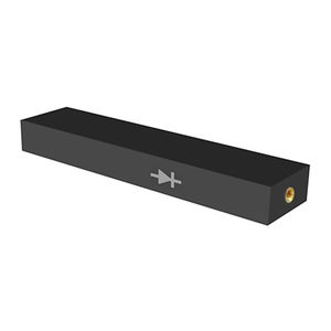
... Halogen-Free and RoHS compliant For surface mounted applications in order to optimize board space Low profile package Built-in strain relief Glass passivated junction Low Inductance Excellent clamping capability ...
Littelfuse

DC voltage: 280, 380, 330, 340 V
Reverse voltage: 4,500, 5,500, 6,000 V
... Diodes can be subdivided into two main classes: Rectifier diodes (standard recovery) and fast diodes. Rectifier diodes are generally used for conversion of AC (alternating current) to ...

DC voltage: 30 V - 200 V
Reverse voltage: 0.4 V - 0.9 V
... quality requirements. The automotive-grade schottky diodes belong to our STPOWER family. STMicroelectronics provides tools which allow designers to quickly find the field-effect rectifier or Schottky diode that best ...
STMicroelectronics

DC voltage: 1.5 V - 3 V
Reverse voltage: 600, 1,250, 650 V
... Renesas' fast recovery diodes offer quick recovery times for rectification purposes in very high-frequency applications. ...

Reverse voltage: 650 V
... Shorter recovery time, enabling high-speed switching. FEATURES: Shorter recovery tim Reduced temperature dependence High-speed switching possible High surge current capability ...
ROHM Semiconductor

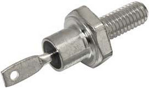
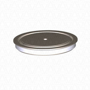
... ; 02641790; 02641800; 02641810; 02643960; 02643340; 02643970; 02638290 Product StatusIn production HousingStud Screw Fit Diodes VRRM / VDRM in V200-1200 IF / IT in A96 IFSM / ITSM in A2000 TechnologyStandard recovery ...
SEMIKRON
DC voltage: 10 V - 120 V
Reverse voltage: 100 V - 1,200 V
... Diodes and Rectifiers - Medium and High Power Diodes Medium and high-power rectifiers are available in several packages including hockey puk capsules and screw-mounted studs, voltage classes are available from 50 V to ...
VISHAY
DC voltage: 0.23 V - 1.18 V
Reverse voltage: 2 V - 250 V
... Low-loss and high current schottky diodes and rectifiers. ...
ON Semiconductor

Reverse voltage: 40 V - 1,600 V
... miniaturization campaign, a new generation of Chip Diodes from Bourns has emerged that offers the capability to provide a silicon diode with minimal packaging overhead. The small signal 0603, 1005 and 1206 Chip Diodes ...
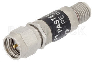
... The PIN diode limiter, which is manufactured by Pasternack Enterprises, is a broadband passive component that is ideal for use in receiver and RF element protection, are also suitable for use in power leveling operations. The unit ...

... Noisecom's noise diodes are the fundamental building blocks for analog noise systems. They are categorized for performance characteristics that enhance their broadband noise output and flat spectral response. All Noisecom noise diodes ...

Reverse voltage: 600 V
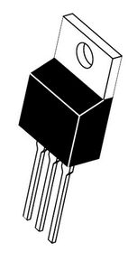
... Description Qspeed™ diodes have the lowest QRR of any Silicon diode. Their recovery characteristics increase efficiency, reduce EMI and eliminate snubbers. Product Highlights Features Now available in TO-263 (D2PAK) ...
Power Integrations

... Configuration:Bidirectional Description:1500W, 100V, 10%, Bidirectional, TVS Family:TVS IPP (A):10.9 IR (µA):1 PPK (W):1500 Package:DO-201 Status:Active TJ Max. (°C):175 Tolerance ± (%):10 VBR Max. (V):110 VBR Min. (V):90 VBR Nom. (V):100 VClamp ...

... Low Forward Voltage Drop • Guard Ring Construction for Transient Protection • Fast Switching Time • Low Reverse Capacitance • Surface Mount Package Ideally Suited for Automated Insertion • Lead, Halogen and Antimony Free, RoHS Compliant "Green" ...
Diodes Incorporated

Reverse voltage: 5 V - 250 V
... TVS Diodes are used to protect sensitive circuit from high-voltage transients.Their p-n junctions have a larger crosssectional area than those of a normal diode,allowing them to conduct large currents to ground without ...
Xiamen SET electronics Co.,Ltd

DC voltage: 200 V - 1,000 V
Reverse voltage: 200 V - 1,000 V
... The CENTRAL SEMICONDUCTOR CMMR1 Series of High Current Density Rectifiers, in a SOD-123F surface mount package are designed for all types of commercial, industrial computer and automotive applications. ...
Central Semiconductor
DC voltage: 4 V
Reverse voltage: 40, 45, 100 V
... Typical Applications Battery-powered devices Output Rectification in DC/DC Converters Polarity Protection Free-wheeling diodes Commercial grade Suffix -Q: AEC-Q101 compliant 1) Suffix -AQ: in AEC-Q101 qualification 1) Features Reverse ...
Diotec

DC voltage: 0.38 V - 0.95 V
Reverse voltage: 20 V - 200 V
... Reverse standoff voltage range from 1,000V to 20,000V Average forward rectified current range from 0.2A to 0.75A ...
Frontier Electronics, Corp.
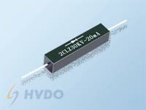
DC voltage: 25 V - 550 V
Reverse voltage: 20 kV - 450 kV
Anshan Suly Electronics Co., Ltd.

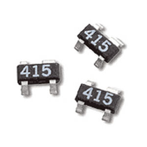
... Features The HSMS-281x family are General purpose, low flicker (1/f) noise schottky diodes.VBR=20 V, CT=1.2pF, RD=15 Ohms, Vf @ 1 mA=410 mV ...
Broadcom
DC voltage: 1.05 V
Reverse voltage: 200, 400 V
... Welding Diode D053-7100 AS ENERGITM are available with forward current IFAV of 7100A and reverse blocking voltages VRRM of 200V, 400V. Series of diodes D053-7100: D053-7100-2-N, D053-7100-4-N. Features of Welding Diodes: ...
AS ENERGI GLOBAL LLC
... Avago Technologies' diodes products include PIN and Schottky diodes for a wide variety of microwave applications including WLAN, WiMAX, infrastructure, handset, SatCom (LNB/DBS-CATV), automotive, military, test & measurement, ...

Reverse voltage: 400, 600, 1,000 V
... Compliant to RoHS Applications DC power supplies Inverters Converters Choppers Ultrasonic systems Freewheeling diodes ...
Nell Power Semiconductor Co. Ltd.

DC voltage: 12 V
Reverse voltage: 12 kV
... Product Features 1. Low leakage, impact resistance, avalanche breakdown protection, etc. 2. Small size, easy to install, suitable for automatic production. 3. High speed switching characteristics, environmental protection process ...
Anshan Leadsun Electronics Co.Ltd
Reverse voltage: 20 kV
... INTRODUCE: Rongtech high voltage silicon rectifier assembly is made of high quality silicon wafer chip and high reliability epoxy resin sealing structure, and through professional testing equipment inspection qualified after to customers. FEATURES: 1.High ...
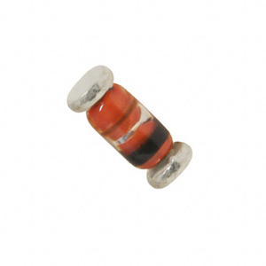
A diode is an electronic component which allows current to flow in only one direction. It can range from a tiny model for an electronic board to larger, screw-in types for high-current use.
ApplicationsDiodes are used principally to rectify alternating current, including in Graëtz bridges for full-wave rectification. They also can protect against reversed polarity in DC circuits. Light-emitting diodes (LED) are used for lighting and displays in optoelectronics. Laser diodes carry information and are found in some lasers and optical amplifiers, in telemetry and in disc readers and writers.
TechnologiesA p-n semiconductor junction is the heart of the diode. It allows current to flow in the forward direction with a small, steady voltage drop. It prevents current flow in the reverse direction up to its breakdown voltage. Zener diodes, which are used as voltage regulators, are not damaged by this reverse flow. TVS diodes use the Zener effect in their avalanche, or surge protection role. Schottky diodes are characterized by reduced DC voltage drop and fast operation. They are used as rapid power rectifiers in converters and switched mode power supplies.
How to chooseChoice will depend primarily on DC power range and reverse breakdown voltage.
the best suppliers