
{{product.productLabel}} {{product.model}}
{{#if product.featureValues}}{{product.productPrice.formattedPrice}} {{#if product.productPrice.priceType === "PRICE_RANGE" }} - {{product.productPrice.formattedPriceMax}} {{/if}}
{{#each product.specData:i}}
{{name}}: {{value}}
{{#i!=(product.specData.length-1)}}
{{/end}}
{{/each}}
{{{product.idpText}}}

... Meco Flex Antenna Plating System (FAP): a unique cost-effective additive process for RFID antenna manufacturing, Flexible PCB and Copper Clad Laminate (CCL). Low Cost RFID Antenna Production Antenna inlays for RFID ...
... edition copper plating process manual; In touch screen you can play the circuit board design sketch after copper plating process; 4. Function characteristics: air-blowing and precoated of copper plating, ...

... With the electroless copper process the PCB normally passes through a total of five process steps to obtain the desired coating thickness of 0.5 µm and more. Depending on the individual process an accelerator level can be integrated if ...
SCHMID

... Direct metallization techniques are used to form a conducting layer in drilled holes before copper plating, as a substitute for electroless copper processes. SCHMID Equipment is available for all commercially available processes based ...
SCHMID

... Levelling process. An extremely finely textured tin layer with a thickness between 0.7 μm and 1 μm is applied to the circuit board surface and into the bore holes. The tin layer protects untreated copper from oxidation; it is a perfect ...
SCHMID
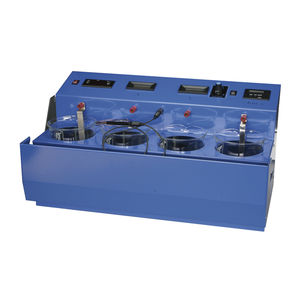
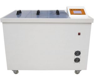
... Six sizes of plating machines are available for plating process, enable both touch-up repairs and bath plating in Pyrex beakers untill 2 liters capacity each. All units have connection for plating ...
the best suppliers