

- Robotics - Automation - Industrial IT
- Industrial Computing
- Dual-core computer-on-module
- MYIR Electronics Limited


- Company
- Products
- Catalogs
- News & Trends
- Exhibitions
Dual-core SoM MYC-J1028XArm® Cortex®-A72 Dual-coreNXPI2C

Add to favorites
Compare this product
Characteristics
- Processor
- dual-core, Arm® Cortex®-A72 Dual-core, NXP
- Ports
- I2C, eDP, SATA III, M.2 Key E, CAN FD, Mini PCIe, M.2 Key B, SPI, UART, WiFi, Ethernet, USB 3.0, DDR4 SO-DIMM, RS-232, RS-485
- Operating system
- Linux® Ubuntu™
- Data storage
- eMMC 16GB, eMMC 8GB, SSD 32GB
- Other characteristics
- embedded, edge computing, GPU, GPIO
- Applications
- industrial, for HMI interface, medical
- Memory size
2 GB
Description
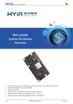
The MYC-J1028X SOM and development board are equipped with the LS1028A processor with a dual-core Cortex™-A72 CPU at 1.5GHz, including Ethernet switches and Ethernet controllers for time-sensitive networking (TSN); Two powerful 64-bit Arm®v8 cores support real-time processing for industrial control; The built-in GPU and LCD controller enable the Human Machine interface (HMI) system to support a new generation of interfaces.
Measuring 45mm by 82mm, the MYC-J1028X SOM is a high-performance embedded core board for industrial and automotive applications. It is based on NXP LS1028A SoC of the Layerscape family and features 1.5 GHz dual Arm Cortex-A72 cores, with integrated 3D GPU for HMI, and a time-sensitive networking (TSN) -enabled Ethernet switch and Ethernet controllers to support converged IT and OT networks. The MYC-J1028X has 2GB DDR4 and supports multiple external memory options including 8GB eMMC (default), QSPI NAND Flash (DNP) and XSPI NOR Flash (DNP). It has 32Kbit EEPROM and one temperature sensor on the rear of the board. A number of peripheral and IO signals are access through one 0.5mm pitch 314-pin MXM 3.0 gold-finger-edge-card connector.
The MYD-J1028X Development Board is using the MYC-J1028X as core controller board and has explored the features of the LS1028A processor to serve as an solid reference design for customer’s development. The base board has brought out rich peripherals through connectors and headers such as one USB3.0 Host, five Gigabit TSN Ethernet, one M.2 Key E based WiFi module interface, one USB 3.0 M.2 Key B based 5G Module interface, one M.2 Key B based SSD Module interface
Catalogs
Other MYIR Electronics Limited products
SOMs


Related Searches
- Intel® Core™ computer
- Industrial computer
- Fanless computer
- HDMI computer
- Embedded computer
- Box computer
- RS-232 computer
- USB computer
- Linux computer
- RS-485 computer
- USB 3.0 computer
- Gigabit Ethernet computer
- WiFi computer
- Mini PCIe computer
- Rugged computer
- DisplayPort computer
- Ethernet computer
- SBC
- RS-422 computer
- 4G computer
*Prices are pre-tax. They exclude delivery charges and customs duties and do not include additional charges for installation or activation options. Prices are indicative only and may vary by country, with changes to the cost of raw materials and exchange rates.
About DirectIndustry
DirectIndustry is a marketplace that offers B2B players a complete experience, from product sourcing to purchase. DirectIndustry is an entity of VirtualExpo Group.
Are you a buyer?
Are you a supplier?