
{{product.productLabel}} {{product.model}}
{{#if product.featureValues}}{{product.productPrice.formattedPrice}} {{#if product.productPrice.priceType === "PRICE_RANGE" }} - {{product.productPrice.formattedPriceMax}} {{/if}}
{{#each product.specData:i}}
{{name}}: {{value}}
{{#i!=(product.specData.length-1)}}
{{/end}}
{{/each}}
{{{product.idpText}}}

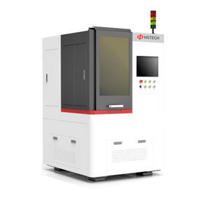
... equipment is used for laser modification and cutting of silicon-based wafers in the semiconductor industry for 8-inch and above chip sealing and testing plants. •High quality There is no damage on the ...
Farley Laserlab
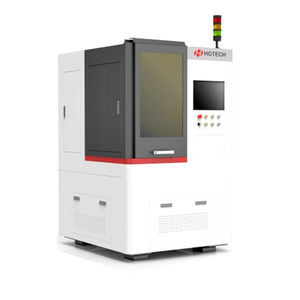
... picosecond laser is used for precision half cutting or full cutting of silicon and compound semiconductor wafers. • High quality Cutting line width is narrow (taking ...
Farley Laserlab
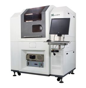
Overall length: 800 mm
Overall width: 1,150 mm
Height: 1,700 mm
... picosecond laser is used for precision half cutting or full cutting of silicon and compound semiconductor wafers. • High quality Cutting line width is narrow (taking ...
Farley Laserlab
X travel: 250 mm
Y travel: 250 mm
Cutting speed: 0.001 m/s - 0.15 m/s
... 1μm 8. Working Table Route:250mm×250mm 9. Max Cutting Size:4 inches 10. Cutting Width:30-50μm 11. Cutting Depth:80-120μm 12. Cutting Speed:1-150mm/s Application: 1. ...
Farley Laserlab
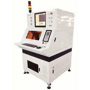
Features: 1. high-quality UV cutting source 2. high cutting quality 3. high cutting reliability 4. small thermal affected zone 5. excellent cutting quality Parameters: ...
Farley Laserlab
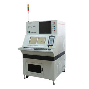
... the rotation axis:20" 6.resolution of XY grating ruler:0.1μm 7. CC positioning precision:1μm 8. cutting linear width:5-10μm 9. cutting depth:20-30μm 10. cutting speed:100mm/s
Farley Laserlab
Please specify:
Help us improve:
remaining