

{{product.productLabel}} {{product.model}}
{{#if product.featureValues}}{{product.productPrice.formattedPrice}} {{#if product.productPrice.priceType === "PRICE_RANGE" }} - {{product.productPrice.formattedPriceMax}} {{/if}}
{{#each product.specData:i}}
{{name}}: {{value}}
{{#i!=(product.specData.length-1)}}
{{/end}}
{{/each}}
{{{product.idpText}}}

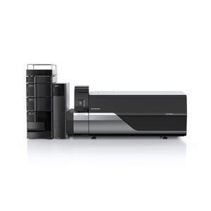
... Scientific™ Nicolet™ iS50 FTIR Spectrometer, featuring purpose-built accessories and integrated software — making it an all-in-one materials analysis workstation. Designed to be highly flexible, the Nicolet iS50 FTIR Spectrometer ...
Thermo Fisher Scientific

... . Key features of the Nicolet Apex FTIR Spectrometers: - Intuitive software — OMNIC Paradigm Software is a powerful analytical tool that empowers researchers and scientists by simplifying spectroscopic data analysis, ...
Thermo Fisher Scientific

... Nicolet Summit X FTIR Spectrometer The Thermo Scientific Nicolet Summit X FTIR Spectrometer can help you reach new heights in productivity, allowing you to accomplish more in less time. It is ideal for both single-user ...
Thermo Fisher Scientific

... The RA800 is a flexible high performance instrument platform. Renishaw can configure it to provide tailored chemical and materials analysis solutions across a range of application areas. Ease of use Simplicity and ease of use make the RA800-series ...

... The FTIR spectrometer ALPHA II combines quality and ease-of-use in a compact shell. The integrated touch PC provides an intuitive user experience and guides you through measurement, evaluation and reporting in a matter of seconds. The ...
Bruker Optics GmbH & Co. KG

... INVENIO is the definitive spectroscopic solution for routine FTIR analysis as well as research and development. It is all you need and so much more: innovative technologies, intelligent design and its new beam path contribute to an unrivalled ...
Bruker Optics GmbH & Co. KG

... MOBILE-IR II is a portable FT-IR spectrometer with full laboratory performance that you can take anywhere. Even on the road, you never have to sacrifice performance or compromise on reliability or spectral quality. With its IP65 protection, ...
Bruker Optics GmbH & Co. KG

... in the aerospace, academic, chemical, pharmaceutical and petrochemical industries. It is the successor to the FTLA2000 spectrometer, also developed by Dr. Buijs and marketed by Bomem inc. since 1985. Smallest footprint. With a vertical, ...
ABB Measurement & Analytics

... MB3600-PH is a FT-NIR spectrometer for the life sciences and pharmaceutical industries designed for QA/QC, research and development and at-line PAT Applications. Since 1997, ABB has supplied the life sciences and pharmaceutical industries ...
ABB Measurement & Analytics

... repeatability performance on the market: precise and reliable data is therefore acquired for optimal control of the process. Our spectrometers provide information needed for process optimization in the refining, chemical, pharmaceutical, ...
ABB Measurement & Analytics

... The CiF3200 sets a new standard in quality control with 2mm precision and multi-color extraction measurement for small and complex samples across diverse industries. Ensure Color Consistency with Data-Driven Color Evaluation Extract Multiple Colors from ...

... shield for enhanced stability and longevity. The SPECTROGREEN MS is an advanced ICP-MS (Inductively Coupled Plasma Mass Spectrometer) that delivers ample analytical headroom to achieve the performance required for routine environmental, ...
SPECTRO Analytical Instruments

Wavelength: 130 nm - 770 nm
... delivers best in class performance in the UV/VUV range The SPECTRO ARCOS inductively coupled plasma optical emission spectrometer (ICP-OES) excels in industrial and academic applications for the most advanced elemental analysis of ...
SPECTRO Analytical Instruments

Wavelength: 165 nm - 770 nm
... SPECTROGREEN inductively coupled plasma optical emission spectrometer (ICP-OES) available in 3 versions: revolutionary Dual Side-On Interface (DSOI), Twin Interface (TI) or Side-On-Plasma (SOP) technology OVERVIEW New revolutionary ...
SPECTRO Analytical Instruments

... Built on the experience and success of the proven Epsilon 3 range of XRF spectrometers, the Epsilon 4 is a multi-functional benchtop XRF analyzer for any industry segment needing elemental analysis from fluorine (F) to americium (Am) ...
Malvern Panalytical

Looking for an easy and economical method for compliant analysis of additives in lubricating oils? Epsilon 1 is the ideal analytical solution. The system is pre-calibrated in the factory and is an out-of the-box solution with guaranteed performance in ...
Malvern Panalytical

Looking for a flexible, yet simple to use, analytical instrument for research and education? Epsilon 1 is the ideal addition to any institution’s analytical equipment. It is capable of simple element identification and quantification to more sophisticated ...
Malvern Panalytical
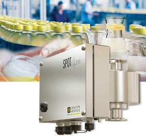
... acknowledged player in spectroscopy and the owner of numerous patents, INDATECH has designed SPOT4Line, the first multi-angle LED spectrometer dedicated to the analysis of any industrial liquid. Based on spectral scattering of light, ...

... reliability and durability of our Pegasus brand in a convenient benchtop unit. Why Choose A Time-Of-Flight Mass Spectrometer? Mass spectrometers are perhaps the greatest tool available for the analytical chemist. ...
LECO
Wavelength: 120 nm - 460 nm
... both the determination of bulk elemental composition, and compositional depth profiling 3. Spectrometer Extension - Choice to add an extension spectrometer, to expand the upper wavelength range from 450 to 850 nm 4. ...
LECO

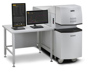
... LECO’s Glow Discharge Spectrometer (GDS) offers you state-of-the-art technology designed specifically for routine elemental determination in most conductive ferrous and nonferrous materials. The GDS900 features improved performance, stability, ...
LECO
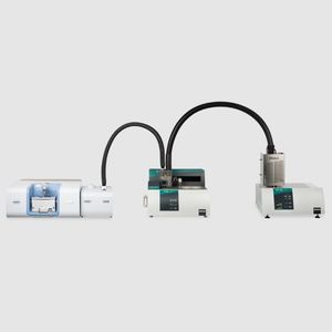
... Product overview
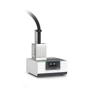
The QMS 505 Aëolos® is a compact quadrupole mass
spectrometer engineered for high-sensitivity gas detection when coupled to thermoanalytical instruments (TGA, STA, DSC, DIL). It integrates a heated capillary ...
NETZSCH Analyzing & Testing
... Highly Sensitive Gas Chromatography-Mass Spectrometry (GC-MS) Coupling to Thermal Analyzers for Precise Identification of Gas Species How to best identify the evolved gases in complex gas mixtures? Separate the gas species first! The primary scope ...
NETZSCH Analyzing & Testing
... Coupling to a Fourier Transform Infrared Spectrometer More than just the sum of its parts Especially in the polymer field as well as in the pharmaceutical and chemical industries, it can be very useful to have knowledge about the ...
NETZSCH Analyzing & Testing
Wavelength: 172 nm - 671 nm
Length: 66.5 cm
Width: 41.5 cm
... Overview
The FOUNDRY-MASTER Smart 2 delivers lab-grade precision for ferrous and non-ferrous metal analysis in a compact, durable format without the complexity or cost of high-end systems.
Built for real-world QA/QC, melt monitoring, ...

Wavelength: 165 nm - 210 nm
... material verification and quality control, or maximise profits in a scrapyard then this oe spectrometer is the solution for you. With the mobile spark spectrometer PMI-MASTER Pro2, you’ll have confidence that you’re getting ...

... XRF analysis (X-ray fluorescence) with the highly flexible and powerful energy-dispersive X-ray fluorescence (EDXRF) spectrometer X-Supreme8000 and LAB-X5000 for quality assurance and process control requirements across a diverse range ...

Wavelength: 400 nm - 2,500 nm
... The DS2500 Analyzers are compact near-infrared (NIR) spectrometers for use in the lab as well as in production. These instruments combine efficiency and intuitive operation with flexibility and robustness. Available product versions ...
Metrohm
... The i-Raman NxG, a next-generation laboratory Raman spectrometer is designed to enhance precision and performance in routine quality control measurements. The i-Raman NxG continues Metrohms tradition of quality, offering advanced features ...
Metrohm

Wavelength: 785 nm
Length: 128 mm
Width: 88 mm
MIRA XTR is an alternative for high power 1064 nm systems. Powered by advanced computational processing, MIRA XTR uses a more sensitive 785 nm laser light along with XTR algorithms to eXTRact the Raman data from the sample fluorescence. MIRA XTR also ...
Metrohm

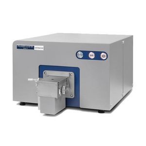
... Quantitative analysis of gas compositions. Pfeiffer Vacuum high end mass spectrometers help you to determine concentrations of gases in gas mixtures. ...
... Interfaces The mass spectrometer achieves an extremely high measuring speed of up to 125 µs/u. It is characterized by maximum sensitivity and a large dynamic range. With the help of the PV MassSpec, the mass spectrometer ...

... Quadrupole mass spectrometers with Faraday detectors are the preferred devices for qualitative analysis of the gas composition in a high-vacuum chamber. Compared with vacuum gauges, quadrupole mass spectrometers offer ...
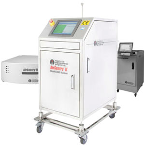
Designed to enhance AMC monitoring programs, the AirSentry II Mobile AMC Monitor is the first truly mobile system for monitoring airborne molecular contamination in cleanrooms. Mobility plays an important part in a strategic airborne molecular contamination ...

The AirSentry II Multi-point AMC Cleanroom Monitor is the most advanced airborne molecular contamination (AMC) system available, using sensitive and responsive ion mobility spectrometry to detect and characterize airborne molecular contamination from ...

... The AirSentry II AMC Monitoring family of ion mobility spectrometers for airborne molecular contamination (AMC) from Particle Measuring Systems detect and alert users to small concentrations or changes in airborne levels of chlorides, ...

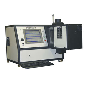
... coolants and water. The SpectrOil 100 Rotating Disc Electrode Optical Emission Spectrometer (RDE-OES) is the eighth generation of the market leading RDE elemental spectrometer. It is widely used in commercial oil laboratories, ...

... SpectrOil M series is the eighth generation RDE Optical Emission Spectrometer for elemental analysis in oil and fuel. It is a compact, rugged, transportable and easy to use optical spectrometer that meets military shock ...
... system that mounts to the spectrometer sample stand and fulfills all the functions of sequentially introducing and removing oil samples and exchanging graphite electrodes. It is self-contained and works independently of the spectrometer ...
... The LCMS-8060NX is a triple quadrupole mass spectrometer with world-class sensitivity and detection speeds. It boasts increased robustness and ease of use as well as Analytical Intelligence to maximize your laboratory’s output. The Culmination ...
Shimadzu France
... Advanced system with AI-assisted operation The Next-Generation Wavelength Dispersive X-Ray Fluorescence (XRF) Spectrometer >12 Mcps Linear count rate for high speed analysis and superb precision with HighSense™ XE detector Uptime Optimal ...
Bruker AXS
... Overview
The LCMS-8065XE is a triple-quadrupole LC-MS/MS mass
spectrometer designed for high sensitivity, high throughput and long-term operational robustness. The system combines StreamFocus ionization, IonFocus ion transmission ...
Shimadzu France

The Analysis Module provides add-on capability for at-line measurement of pH and optionally, Raman spectroscopy, for Ambr® 15 and Ambr® 250 High Throughput bioreactors. The pH measurement automates initial bioreactor vessel pH sensor calibration and subsequent ...
Sartorius AG

... The Agilent 240FS AA is a Fast Sequential atomic absorption spectrometer that can double sample throughout and dramatically reduce running costs. Able to handle multi-element suites with ease, the Agilent 240FS AA system is ideal for ...
Agilent Technologies - Life Sciences and Chemical
... The SCIEX 7500+ system is a triple quadrupole engineered to maintain our highest sensitivity for up to twice as long in complex matrices. Have the confidence to tackle even the most challenging studies and run continuously at the highest level of performance When ...
SCIEX

... Hand-held Atomic Fluorescence Spectroscopy Mercury Vapor Analyzer The Jerome® J505 Mercury Vapor Analyzer is a portable fluorescence spectroscopy analyzer, which allows the detection cell to be simpler, smaller, lighter weight and more durable than ...

Width: 95 cm
Height: 64 cm
Engineered with an array of exciting technological advances, the PinAAcle™ 900 atomic absorption (AA) series offers a variety of configurations and capabilities to deliver exactly the level of performance you need. And no matter which model you select, ...
PerkinElmer

... is pre-optimized to work with your samples, without the sample-specific or user adjustments typical of traditional mass spectrometers. For the first time, any analytical scientist can consistently generate the highest quality mass spectral ...
Waters
Wavelength: 200 nm - 1,100 nm
... system that integrates a spectrometer and optical detector into a single unit. High sensitivity enables spectrum acquisition by positioning an optical fiber near the sample without a dedicated light collection system. The spectrometer ...
HAMAMATSU
A spectrometer can measure the spectral composition of light including intensity, frequency and wavelength. When analyzing atomic and ionic characteristics, intensity is a function of mass.
ApplicationsThese instruments are used for both quantitative and qualitative analyses. They often serve as chromatographic detectors.
TechnologiesThe most common are optical spectrometers, which operate in the visible spectrum. Some use a prism to break light into its constituent colors, or wavelengths. Grating models include an optical diffraction component which splits light into various beams.
Other instruments operate in the non-visible spectrum. Infrared spectrometers employ infrared light to perform qualitative and quantitative material analysis. Atomic absorption spectrometers (AAS) are used to analyze metals and metalloids.
the best suppliers