

{{product.productLabel}} {{product.model}}
{{#if product.featureValues}}{{product.productPrice.formattedPrice}} {{#if product.productPrice.priceType === "PRICE_RANGE" }} - {{product.productPrice.formattedPriceMax}} {{/if}}
{{#each product.specData:i}}
{{name}}: {{value}}
{{#i!=(product.specData.length-1)}}
{{/end}}
{{/each}}
{{{product.idpText}}}
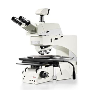
... on the latest LED technology and is fully integrated into the microscope. The low heat radiation and integration into the stand ensures that there is an optimal airflow around the microscope. The long lifetime yet extremely ...

... on the latest LED technology and is fully integrated into the microscope. The low heat radiation and integration into the stand ensures that there is an optimal airflow around the microscope. The long lifetime yet extremely ...
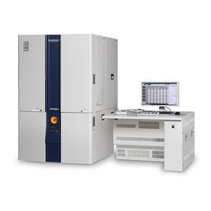
Magnification: 3,000,000 unit
Resolution: 0.8, 0.4, 1.2 nm
... The SU9000 II is a combination of surface-imaging SEM and intrinsic structure-resolving scanning transmission microscope (STEM) optimised for extreme resolution. This is made possible by the unique electron optics of ...

Weight: 9.5 kg
Length: 657 mm
Width: 251 mm
... Modular Motorised and Manual Upright Microscopes Superb Nikon CFI60-2 optics provide excellent images to both eyepieces and to Nikon’s digital imaging cameras with analysis software. The universal microscope design ...
Nikon Metrology

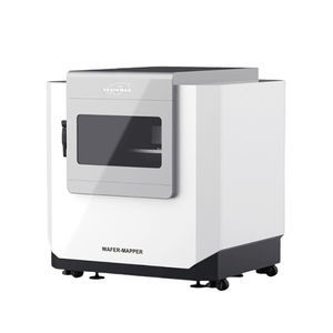
... 300 AUTO WAFER is a product line developed for in line production control of bonded wafers. Its is compatible with clean room class 10. The main application is detection of voids, inclusions and delaminated areas at ...

Resolution: 5 µm
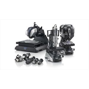
... feature resolution and 3 linear axes with precision ball bearing Triax – Low-noise measurements down to fA levels • Stereo microscope: 15x–100x magnification with large field-of-view and camera-ready c-mount • Four triax probe arms ...
FORMFACTOR
Magnification: 2,500 unit - 6,000 unit
Weight: 10.8 kg
... features. Capture Details That Other Microscopes Overlook Combining lighting from multiple directions allows for clear observation of subtle surface conditions that were impossible to see with optical microscopes ...
Resolution: 0.02 µm
... The Atomic Force Microscope ( wafer-level AFM) is a high-resolution scanning probe instrument designed to characterize three-dimensional surface morphology and multifunctional properties of conductors, semiconductors and ...
the best suppliers