

- Metrology - Laboratory
- Metrology and Test Equipment
- Volume measuring system
- Chotest Technology Inc.


- Company
- Products
- Catalogs
- News & Trends
- Exhibitions
Thickness measuring machine BOKI_1000volumeoptical3D


Add to favorites
Compare this product
Characteristics
- Measured physical value
- thickness, volume
- Technology
- optical, 3D
- Measured material
- for small parts, optical lens, for wafers, for glass
- Applications
- for industrial applications, for electronics, laboratory
- Other characteristics
- high-precision, non-contact
Description
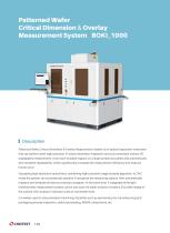
Patterned Wafer Critical Dimension & Overlay Measurement System is an optical inspection instrument that can perform both high-precision XY plane dimension inspection and sub-nanometer surface 3D topography measurement. It can scan multiple regions on a large surface accurately and automatically with excellent repeatability, which significantly increases the measurement efficiency and reduces human error.
Equipping high-resolution optical lens, combining high-precision image analysis algorithm, in CNC mode the system can automatically position & recognize the measuring objects, then automatically measure and evaluate all sizes according to program. At the same time, it integrates white light interferometry measurement system, which can scan the wafer surface to create a 3D profile image of the surface, then analyze Z-direction sizes in nanometer level.
It is widely used in ultra-precision machining industries such as semiconductor manufacturing and packaging process inspection, optical processing, MEMS components, etc.
Application
Overlay Offset Measurement
Key Dimensions Measurement
3D Dimensions Measurement
Etch Depth Measurement and Profile Analysis
Laser Groove Depth and Width Measurement
VIDEO
Catalogs

Other Chotest Technology Inc. products
Microscopic Surface


Related Searches
- Test machine
- Chotest measuring instrument
- Chotest measuring system
- Automatic test machine
- Industrial test machine
- Vertical test machine
- Laboratory test machine
- Digital measuring device
- Precision test machine
- Portable measuring device
- Chotest industrial measuring instrument
- Chotest automatic measuring system
- Quality control test machine
- Chotest optical measuring system
- Chotest high-precision measuring system
- Test machine for the automotive industry
- Chotest measuring system for industrial applications
- Digital test machine
- Touch probe head
- Chotest benchtop measuring instrument
*Prices are pre-tax. They exclude delivery charges and customs duties and do not include additional charges for installation or activation options. Prices are indicative only and may vary by country, with changes to the cost of raw materials and exchange rates.
About DirectIndustry
DirectIndustry is a marketplace that offers B2B players a complete experience, from product sourcing to purchase. DirectIndustry is an entity of VirtualExpo Group.
Are you a buyer?
Are you a supplier?