
{{product.productLabel}} {{product.model}}
{{#if product.featureValues}}{{product.productPrice.formattedPrice}} {{#if product.productPrice.priceType === "PRICE_RANGE" }} - {{product.productPrice.formattedPriceMax}} {{/if}}
{{#each product.specData:i}}
{{name}}: {{value}}
{{#i!=(product.specData.length-1)}}
{{/end}}
{{/each}}
{{{product.idpText}}}

The CEX series platform is an easy to implement surface mount solution for gain variation over frequency. Various configuration options including different frequency bands, slope direction and slope magnitude are available to support multiple markets ...

... The HR-CTX high frequency termination series offers excellent broadband performance up to 64GHz and unrivalled power rating capability up to 5 Watts in a small 0404 package. Its small footprint allows customers to save space and weight on the board, ...

... The PAC1921 is a dedicated power-monitoring device with a configurable analog output that can present power, current or voltage. All information is also provided on the 2-wire/I2C© compatible interface. The PAC1921 is designed for power measurement ...
Microchip Technology Inc.
... Product summary
The ADC32RF72 is a 16-bit, dual-channel, non-interleaved RF-sampling analog-to-digital converter (ADC) operating up to 1.5 GSPS. It targets very high SNR and ultra-low noise spectral density, delivering −163.7 dBFS/Hz (improvable ...
Texas Instruments
The ADPL44002 is a CMOS, low dropout (LDO) linear regulator that operates from 2.7V to 40V and provides up to 200mA of output current. This high input voltage LDO is ideal for the regulation of high performance analog and mixed signal circuits operating ...
Analog Devices
The AS7058 is an integrated multi-vital sign monitoring device, which provides a complete photoplethysmogram (PPG), electrocardiogram (ECG), body impedance (BioZ), and electrodermal activity (EDA). PPG measures the pulse rate or blood oxygen by sampling ...

... Smart metering Analog Front End (AFE) ICs offer high accuracy when measuring DC and AC energy down to extremely low currents typical of home appliances in standby mode. ...
... I2C-Bus Controller and Bridge ICs Continuing our leadership in I2C-bus devices, we offer a vast portfolio of I2C logic products for communication and protocol conversion. These solutions support many systems using SMBus, advancedTCA ...
NXP Semiconductors
... Greater Efficiency from Power Management Samsung Power IC solutions rethink the way products work to bring efficient energy innovations to the new mobiles, wearables and IoT applications. Brainy Management for Perfect PowerExpert ...
Samsung Semiconductor

The ET1100 EtherCAT ASIC offers a cost-effective and compact solution for realizing EtherCAT slaves. It processes the EtherCAT protocol in the hardware and therefore ensures high-performance and real-time capability, independent of any downstream slave ...

This 25Gbps photodiode chip, which is top-illuminated high data rate PIN photodiode chip, with active area is Φ32μm. Its features have high responsivity, low capacitance, low dark current and excellent reliability, mainly combination with high performance ...
PHOGRAIN TECHNOLOGY(SHENZHEN) CO., LTD.

This 25Gbps photodiode chip, which is top-illuminated high data rate PIN photodiode chip, with active area is Φ32μm. Its features have high responsivity, low capacitance, low dark current and excellent reliability, mainly combination with high performance ...
PHOGRAIN TECHNOLOGY(SHENZHEN) CO., LTD.

This high data rate 10Gbps photodiode chip is InGaAs/InP PIN structure and top-illuminated. Features is high responsibility, low capacitance, low dark current, active area size is Φ50μm, anode and cathode bond pad on top for TO-CAN package wire-bonding. ...
PHOGRAIN TECHNOLOGY(SHENZHEN) CO., LTD.
... High Efficiency Off-line CV/CC QR Flyback Switcher IC with Integrated 725 V Primary MOSFET, Synchronous Rectification and Integrated Secondary-Side Control The InnoSwitch3-TN family dramatically increases the efficiency of auxiliary ...
Power Integrations
... The CMX983 is an Analogue Front End (AFE) IC that bridges the gap between a digital radio’s RF section and the DSP/FPGA. Specifically designed to meet the needs of a Software Defined Radio (SDR). It is suitable for radio systems employing ...
CML Microcircuits
... Cirrus Logic’s flagship CS3318 is an eight-channel, high-voltage, digitally controlled analog volume control IC that is the benchmark for audio quality, showcasing 127 dB dynamic range. The CS3318 operates from a ±9 V power supply, with ...
Cirrus Logic
The AL3565 is a Power Management Integrated Chip (PMIC) with three programmable DC-DC converters via a simple one wire digital control to power supply bias 500mA AMOLED (Active Matrix Organic Light Emitting Diode) panel requiring three supply rails, VPOS, ...
The S Series is the worlds’ first software-defined platform that massively integrates 4G, 5G and AI into a single chip. Completely software programmable, the S Series leverages over-the-air upgradeability for new features rollout, 4G to 5G transition, ...

The MCP6486/6R/6U/7/9 series of operational amplifiers have low input bias current and rail-to-rail input and output operation. This family is unity gain stable and has a gain bandwidth product of 10 MHz (typical). These devices operate with a single-supply ...
Atmel
... High performance optical head transmitter for DSP-based 1.6Tbps data center optical modules Key Features Silicon photonics monolithically integrated laser and modulators 224Gbps PAM4 modulators ...
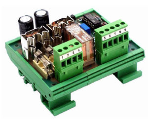
... EM-12A DC-motor control unit is designed for use in industry and automation applications in power range of 0...200 W. With EM-12A DC-motor can be controlled easily and economically. EM-12A includes many adjustments and various connection choices. Inbuilt ...
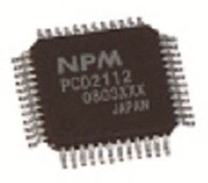
... Nippon Pulse offers a single-axis control chip, the PCD2112. A small molded package 48-pin QFP, the PCD2112 packs a powerful control set into a 7mm x 7mm chip. The PCD2112, which has Serial Peripheral Interface Bus (SPI) interface, can offer a custom ...
Nippon Pulse
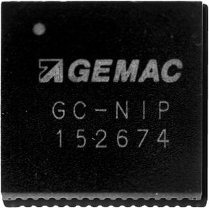
... system, a resolution of up to 22 bit can be achieved. Input and output of the GC-NIP are designed for 3.3V interfaces. The IC comprises six instrumentation amplifiers with adjustable gain factors. Encoders with voltage interface or ...
AMAC ASIC - und Mikrosensoranwendung Chemnitz GmbH
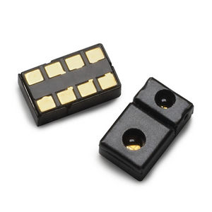
... Proximity sensors detect the presence or absence of an object. Examples of proximity sensor usage include detecting an out-of-paper condition in a printer or a mobile phone screen that dims to save battery life when placed near a face. Avago Proximity ...
... The Allegro™ A1377 programmable linear Hall-effect sensor IC is designed for applications that require high accuracy and high resolution without compromising bandwidth. The A1377 employs segmented, linearly interpolated temperature compensation ...
ALLEGRO MICROSYSTEMS
... Multi Quantum Well Distributed Feedback Laser Direct modulation beyond 2.5Gbps Uncooled operation from -20°C to +85 °C Designed for Telcordia GR-468 Small farfield Applications PON, ACCESS, Optical Ethernet, SDH ...
Guilin GLSUN Science and Tech Group Co., Ltd

... Applications Programmable sensor interface for optical and magnetic position sensors Linear gauges and incremental encoders Linear scales Features PGA inputs to 500 kHz for differential and single-ended sensor signals Selectable adaptation to voltage ...
the best suppliers