
{{product.productLabel}} {{product.model}}
{{#if product.featureValues}}{{product.productPrice.formattedPrice}} {{#if product.productPrice.priceType === "PRICE_RANGE" }} - {{product.productPrice.formattedPriceMax}} {{/if}}
{{#each product.specData:i}}
{{name}}: {{value}}
{{#i!=(product.specData.length-1)}}
{{/end}}
{{/each}}
{{{product.idpText}}}
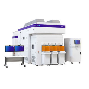
... The 3935 and 3920 EP broadband plasma defect inspection systems support wafer-level defect discovery, yield learning and inline monitoring for ≤5nm logic and leading-edge memory design nodes. With a light source that produces super resolution ...
KLA Corporation
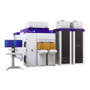
... High-productivity broadband inspection for diverse substrates (Si, SiC, GaN, glass) and wafer sizes (150/200/300mm) with DesignWise® and DefectWise® AI.
KLA Corporation
... noise sensor to capture critical defects across a range of process layers and device types. NanoPoint™ technology focuses inspection on pattern areas at high risk for reliability failures, delivering actionable defect data that helps ...
KLA Corporation
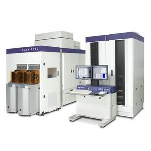
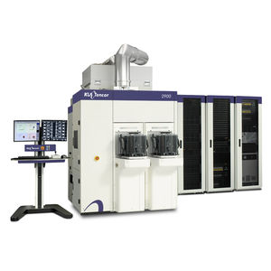
... The Puma™ 9980 laser scanning inspection system incorporates multiple sensitivity and speed enhancements that enable capture of critical defects of interest (DOI) at throughputs required for high volume manufacturing for 1Xnm advanced ...
KLA Corporation
... comprising the latest-generation CIRCL5 system include: front side wafer defect inspection; wafer edge defect inspection, profile, metrology and review; backside wafer defect inspection and review; and, ...
KLA Corporation
... within fabs. Unpatterned wafer surface inspection system with DUV sensitivity and high throughput for IC, substrate and equipment manufacturing at the sub 1Xnm design nodes. Unpatterned wafer surface inspection system ...
KLA Corporation
... supports wafer and chip manufacturing for wide-bandgap semiconductors. It provides high resolution images of defects and uses machine-learning automatic defect classification to produce an accurate defect pareto. The data generated by ...
KLA Corporation
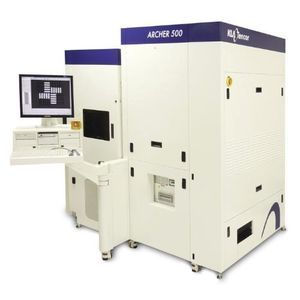
The Archer™ 800 overlay metrology system provides accurate feedback of on-product overlay error for fast technology ramps and stable production of leading-edge memory and logic devices. Wavelength tunability and optimization per layer with nanometer-level ...
KLA Corporation
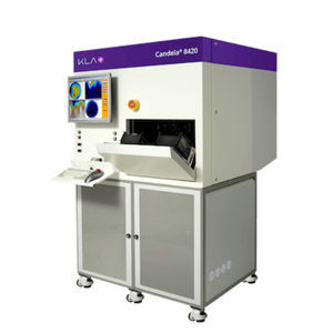
... DOI). Full-surface coverage is achieved in minutes, with the Candela 8420 surface defect inspection system to produce high resolution imaging and automated inspection reporting with defect classification and wafer maps. ...
KLA Corporation
... surface and photoluminescence defect inspection for GaN wafers, detecting and classifying GaN dislocations, pits and holes for GaN reactor defect control. Power applications include SiC based transparent wafer inspection ...
KLA Corporation