
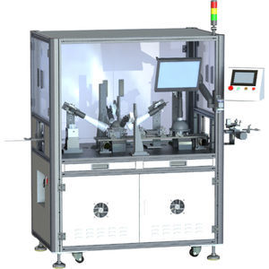
{{product.productLabel}} {{product.model}}
{{#if product.featureValues}}{{product.productPrice.formattedPrice}} {{#if product.productPrice.priceType === "PRICE_RANGE" }} - {{product.productPrice.formattedPriceMax}} {{/if}}
{{#each product.specData:i}}
{{name}}: {{value}}
{{#i!=(product.specData.length-1)}}
{{/end}}
{{/each}}
{{{product.idpText}}}
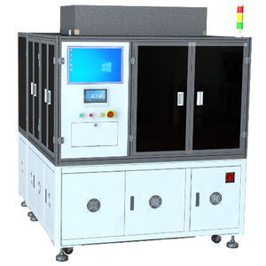
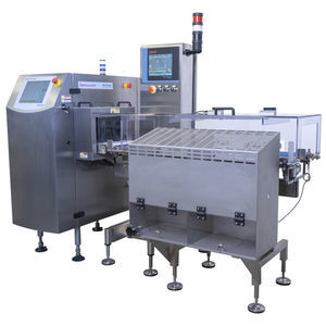
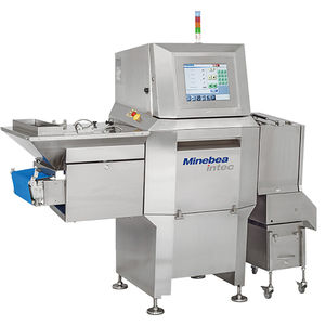
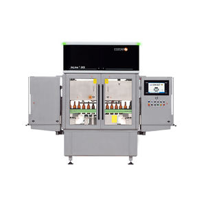
Inspection range width: 340 mm - 340 mm
... checkweigher.
X-ray inspection available as combos
NextGuard C330 X-ray inspection as combo
Sensitivity: Very high
Case width: 340 mm
Technology: X-ray
inspection; ...

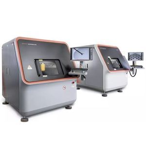
... is Waygate Technologies' easy to use entry-level microfocus X-ray inspection (AXI) system with strong performance that is designed for the special needs of the high-resolution inspection of electronic assemblies, components ...
Waygate Technologies
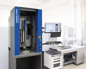
... wide spectrum of 2D and 3D offline inspection tasks: R&D, failure analysis, process and quality control. The Phoenix|x-ray X|act inspection software offers easy to program CAD based µAXI ensuring automated inspection ...
Waygate Technologies

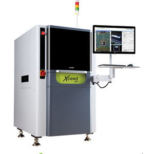
... Industrial Scanner featuring unparalleled flexibility and efficiency Advances in inspection technology have yielded a highly versatile high-resolution system for 2D X-ray inspection and 3D computed tomography (microCT ...
Waygate Technologies

... dents and so on. This Is one of the most important inspections at the end of the production process. It can be simply integrate with offering accurate measuring results. It is ideal for all common TU machine, with optical ...

... is detected by cameras. The measuring system contains fully automated integrated calibrations. The patented process of the calibration takes approximately 5 minutes. The visualization software of the profilometer contains ...

... adaptive dynamic masking, and high resolution enable automated 100 % inspection of bores within the required cycle time of the production process. The systems allow a fast inspection of the complete bore surfaces, as ...

... Optical inspection of plane surfaces The Visionline F sensors are specially designed for the automatic inspection of plane surfaces. Thanks to the fly-over technology, image acquisition takes place in the movement ...
... Standalone systems for optical bore inspection The systems for optical bore inspection in the Visionline V200 series deliver reliable and reproducible inspection results without operator influence. ...
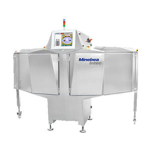
... X-ray inspection system - Dylight The X-ray inspection system Dylight guarantees extremely high levels of safety for your packaged food. This true ‘Plug and Play’ solution combines all functions in one compact unit. Extremely ...
Minebea Intec GmbH
... X-ray inspection system - Dymond Bulk Dymond Bulk guarantees precise X-ray inspection of bulk materials in the food industry. Foreign bodies such as stones or metal are consistently detected and removed from the material ...
Minebea Intec GmbH
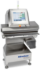
Inspection range height : 800 mm - 1,000 mm
... X-ray inspection system Dymond - Dymond S The Dymond S side shooters offer reliable detection of foreign objects in tall, upright packaging. The compact hygienic design, interfaces and reliable image processing at high speeds allow for ...
Minebea Intec GmbH
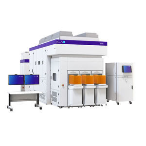
... The 3935 and 3920 EP broadband plasma defect inspection systems support wafer-level defect discovery, yield learning and inline monitoring for ≤5nm logic and leading-edge memory design nodes. With a light source that produces super resolution ...
KLA Corporation
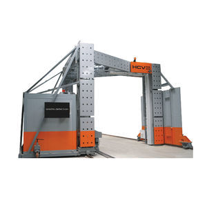
... Gantry inspection system The HCVG provides side view images of inspected vehicles, offering material discrimination for easy assessment of cargo and vehicle contents in a single scan. The HCVG X-ray system uses a single scan to screen ...
Smiths Detection

... scanners for high-resolution inspection of components ranging from miniature plastic connectors to aluminium castings. Systems are intended for R&D, failure analysis and production quality control with configurations for inspection ...
Nikon Metrology
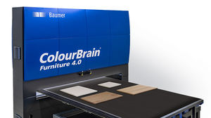
... The inspection system ColourBrain® Furniture 4.0 is the technology leader in the double-sided inspection of foil-coated, melamine-coated and lacquered furniture panels. The outcome are impressive inspection ...
Baumer Inspection

... experience in camera visual inspection with HVLD (High Voltage Leak Detection) system. Furthermore these models are equipped with an integrated labelling unit for the products which passed all the previous inspections. The ...
Marchesini Group
... optimally tailored to the inspection machine and all components are perfectly matched with each other. These are the preconditions for ideal inspection results." Your benefits No glass-to-glass contact No ...
Körber Pharma

... Last generation of sidewall inspection machine Universal and flexible: adapted to all markets and all line configuration Simple and Efficient: Suitable for all users and all types of detections Selective and productive: ...
Tiama Group
... screen High energy X-ray High energy X-ray enable a broad range of inspection target (80 kV). Can be used for the inspection of thick metals, shoes soles etc. Enlarged in-tunnel inspection area L-shaped ...
Rigaku
Inspection range width: 500 mm
Inspection range height : 250 mm
Convey weight capacity: 25 kg
... production line requirements
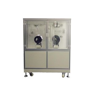
... , length, fiber diameter, number of bump defects. Specifications ● Adaptive fiber diameter range: Ø 0.10~Ø 0.250mm ● Machine winding speed: 0~800r/min ● Length error: ≤0.3% ● Tension control range: 8~40g ● Tension fluctuation ...
... Appliction: Thickness and warpage measurement for unpatterned wafer The 3D shape based on the upper and lower surfaces of the wafer is reconstructed by non-contact measurement. The powerful measurement and analysis software ensures the stable calculation ...

Inspection range height : 300 mm
Convey weight capacity: 15 kg
The nanoVoxel-2000 system is a high-performance imaging system that uses a sealed X-ray source. The X-ray source is maintenance-free and the sample chamber can accommodate large -size samples, is capable of expanding the in-situ loading device, and can ...
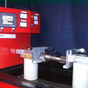
... rolling, welding and other defects makes them an essential in industries tool such as the steel, automotive, aviation, rail, shipbuilding and chemical sectors. Robustness and reliability: TemaFlux MPI horizontal units are robust and ...

... foundations or excavations, and are easily movable with a forklift. Ergonomics and accessibility: rotating tables for parts inspection, with variable dimensions and capacity. Safety and Maintenance: •Stainless steel liquid collection ...
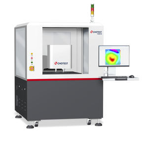
... Based on 3D laser line scanning equipment, the defect inspection and contour metrology of metal plate are completed Detect global warpage, standard burr, and other defects Technology Advantages Scanning Accuracy = 0.0005mm ...
... Self-developed efficient algorithm model can quickly output inspection results, in line with the highest production tempo, to avoid causing bulk scrapping - Based on high-precision inspection results, the pieces are ...
... efficiency, stability and consistency of quality testing Effect Taking place of manual inspection, the efficiency can be 20 times higher than manual inspection. It can output quantitative standards and improve the ...

... 3D SPI Laser Line Scan Method Fastest Inspection Speed in the Industry Real 3D Image Inspection Irrelevant to Color, Material, Surface Roughness Automated Measurement of PCB Warpage Automated Compensation ...
PARMI Europe GmbH

Inspection range height : 0 mm - 65 mm
... Technology: 3D AOI using laser line scan method
PARMI Europe GmbH
... user needs: SPI (Solder Paste Inspection) / AOI (Automated Optical Inspection) / CCI (Conformal Coating Inspection).
PARMI Europe GmbH

Output power: 60 W - 150 W
Inspection range width: 0 mm - 240 mm
Inspection range height : 0 mm - 120 mm
... inside the machine is reduced due to moisture or dust. It can prolong the lifetime of its electric boards, switches, etc. Comparison of waterproof range ● Due to IP66, it is washable and can be kept sanitary. It prevents your production ...
SYSTEM SQUARE Inc.

Output power: 60 kW - 150 kW
Inspection range width: 220 mm
Inspection range height : 120 mm
... with the new X-ray sensor (SX2-2353HW), a further high-sensitivity inspection has been achieved compared with the SYSTEM SQUARE standard system (SX2-2554W). By comparing the inspection images, it can be confirmed that ...
SYSTEM SQUARE Inc.

Output power: 60 kW - 150 kW
Inspection range width: 0 mm - 240 mm
Inspection range height : 0 mm - 120 mm
... SX2-2554HW Highly stable relative mass inspection achieved with a new X-ray sensor Stable mass inspection achieved with a new X-ray sensor The relative mass inspection can be made stably even for ...
SYSTEM SQUARE Inc.
Output power: 100 W
Inspection range width: 110 mm - 280 mm
Inspection range height : 0 mm - 120 mm
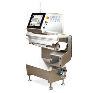
... Efficient product even in limited spaces. The Dylight series represents the entry-level range of vertical machines. At an affordable price, it offers the most advanced and rational technical solutions. It features a versatile all-in ...
DYLOG HITECH

... Taymer’s Offline medical product inspection systems leverage the benefits of Taymer’s inspection software over discrete product lengths. The offline Medical Surface Inspection machines ...

... A high-speed, precision inspection machine for 100% near-line or inline gear inspections. Non-contact 3D Gear Inspection System ZeroTouch® ZTG is a non-contact gear inspection ...
DWFRITZ Metrology
... Simply detecting more: X-ray assisted empty bottle inspection based on the HEUFT SPECTRUM II. The HEUFT InLine II IXS achieves simply more precision during the complete all-around inspection of empty bottles. For this ...
HEUFT SYSTEMTECHNIK
the best suppliers