

- Metrology - Laboratory
- Laboratory Equipment
- Scanning electron microscope
- Hitachi High-Tech Europe GmbH


- Company
- Products
- Catalogs
- News & Trends
- Exhibitions
Scanning electron microscope TM4000PlusIIImeasuringfor analysistopography


Add to favorites
Compare this product
Characteristics
- Type
- scanning electron
- Technical applications
- for analysis, measuring
- Observation technique
- atomic number contrast, topography
- Configuration
- benchtop, compact
- Detector type
- back-scattered electron, secondary electron
- Other characteristics
- motorized, digital camera, high-resolution, automated, cost-effective, high-contrast, high-magnification, image-processing, simple installation, asbestos identification, earth sciences, for nanotechnology, for integration microscope and profilometer, for polished samples, variable pressure scanning, with profiler function, for flat samples, topography, for air/liquid use
- Magnification
Min.: 10 unit
Max.: 250,000 unit
- Weight
53 kg, 55 kg
(116.8 lb, 121.3 lb)- Length
614 mm, 617 mm
(24.2 in, 24.3 in)- Width
330 mm
(13 in)- Height
547 mm
(21.5 in)
Description
High-performance tabletop SEM for flexible imaging needs in academia and industry.
The Hitachi TM4000PlusIII scanning electron microscope offers a compact, user-friendly solution for imaging and elemental analysis. Designed for a range of users - from research labs to industrial quality control - this new tabletop SEM gives you reliable imaging capabilities without the costs and space requirements of a traditional SEM.
Why choose the TM4000PlusIII?
Whether you're a research scientist looking to deepen your understanding of materials or a quality control manager striving for consistent results, the TM4000PlusIII is built to meet your needs.
This microscope brings the power of scanning electron microscopy into an accessible, tabletop design. It combines ease of use with powerful features for imaging, navigation, and analysis.
With automated functions to streamline repetitive tasks, high signal-to-noise ratio for clear imaging, and an intuitive user interface, this SEM makes electron microscopy more approachable and productive then ever.
Features and benefits
Automation for consistent and reliable imaging
Auto-focus, brightness, and contrast ensure consistent results across multi-user environments.
Automated stage movement, magnification adjustments, and image capture simplify operation for inexperienced users.
Optional tools like Multi-Zigzag, Python scripting, and EM-Flow Creator enable reproducible workflows without coding skills.
Well-resolved, high depth-of-focus and multiple-mode imaging
Precise, contrast-rich imaging at 5, 10, or 15 kV.
Backscattered and secondary electron detectors provide compositional, topographical, and surface details.
Mixed output from both detectors delivers comprehensive imaging insights in a single image.
Enhanced imaging flexibility and elemental analysis
Optional integrated EDX for material composition analysis with 30 mm² or 60 mm² sensors.
Switch seamlessly between imaging and elemental mapping for comprehensive sample studies.
Compatible with AZtecLiveLite for efficient, high-throughput analysis.
Navigate with ease using optical caméra intégration
Integrated high-resolution optical camera provides a zoomable map overview of samples.
Pair optical images with SEM snapshots for precise navigation and seamless operation.
Idéal for educational and non-conductive samples
Low-vacuum functionality ensures clear imaging of delicate or non-conductive samples without extensive preparation.
Suitable for educational settings, allowing students and early-career researchers to explore electron microscopy easily.
Maintenance planning with filament monitoring
Tracks filament usage and projects remaining lifespan for proactive maintenance planning.
Ensures uninterrupted workflows and minimizes downtime in labs with multiple users.
- Automation for consistent and reliable imaging
- Optional elemental analysis
- Ideal for both conductive and non-conductive samples
- Well-resolved, high depth-of-focus and multiple-mode imaging
- Navigate with ease using optical camera integration
- Maintenance planning with filament monitoring
The Hitachi TM4000PlusIII scanning electron microscope offers a compact, user-friendly solution for imaging and elemental analysis. Designed for a range of users - from research labs to industrial quality control - this new tabletop SEM gives you reliable imaging capabilities without the costs and space requirements of a traditional SEM.
Why choose the TM4000PlusIII?
Whether you're a research scientist looking to deepen your understanding of materials or a quality control manager striving for consistent results, the TM4000PlusIII is built to meet your needs.
This microscope brings the power of scanning electron microscopy into an accessible, tabletop design. It combines ease of use with powerful features for imaging, navigation, and analysis.
With automated functions to streamline repetitive tasks, high signal-to-noise ratio for clear imaging, and an intuitive user interface, this SEM makes electron microscopy more approachable and productive then ever.
Features and benefits
Automation for consistent and reliable imaging
Auto-focus, brightness, and contrast ensure consistent results across multi-user environments.
Automated stage movement, magnification adjustments, and image capture simplify operation for inexperienced users.
Optional tools like Multi-Zigzag, Python scripting, and EM-Flow Creator enable reproducible workflows without coding skills.
Well-resolved, high depth-of-focus and multiple-mode imaging
Precise, contrast-rich imaging at 5, 10, or 15 kV.
Backscattered and secondary electron detectors provide compositional, topographical, and surface details.
Mixed output from both detectors delivers comprehensive imaging insights in a single image.
Enhanced imaging flexibility and elemental analysis
Optional integrated EDX for material composition analysis with 30 mm² or 60 mm² sensors.
Switch seamlessly between imaging and elemental mapping for comprehensive sample studies.
Compatible with AZtecLiveLite for efficient, high-throughput analysis.
Navigate with ease using optical caméra intégration
Integrated high-resolution optical camera provides a zoomable map overview of samples.
Pair optical images with SEM snapshots for precise navigation and seamless operation.
Idéal for educational and non-conductive samples
Low-vacuum functionality ensures clear imaging of delicate or non-conductive samples without extensive preparation.
Suitable for educational settings, allowing students and early-career researchers to explore electron microscopy easily.
Maintenance planning with filament monitoring
Tracks filament usage and projects remaining lifespan for proactive maintenance planning.
Ensures uninterrupted workflows and minimizes downtime in labs with multiple users.
VIDEO
Catalogs
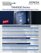
TM4000 Series
2 Pages
Other Hitachi High-Tech Europe GmbH products
Table Top / Compact SEM


Related Searches
- Hitachi microscope
- Hitachi laboratory microscope
- Inspection microscope
- Tabletop microscope
- Digital camera microscope
- Measuring microscope
- Hitachi analysis microscope
- Industrial microscope
- Hitachi automated microscope
- Hitachi high-resolution microscope
- Bright field microscope
- Compact microscope
- Materials research microscope
- Metallurgical microscope
- Quality control microscope
- Research microscope
- Black field microscope
- Ergonomic microscope
- Specimen maker
- 3D microscope
*Prices are pre-tax. They exclude delivery charges and customs duties and do not include additional charges for installation or activation options. Prices are indicative only and may vary by country, with changes to the cost of raw materials and exchange rates.
About DirectIndustry
DirectIndustry is a marketplace that offers B2B players a complete experience, from product sourcing to purchase. DirectIndustry is an entity of VirtualExpo Group.
Are you a buyer?
Are you a supplier?
© 2026 All rights reserved - Terms - Privacy policy - General Terms - Manage cookies - 鄂ICP备2026053537号-2 -