

- Metrology - Laboratory
- Laboratory Equipment
- Electron microscope
- Hitachi High-Tech Europe GmbH


- Company
- Products
- Catalogs
- News & Trends
- Exhibitions
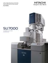
Field emission scanning electron microscope SU7000for analysisin-situBF-STEM


Add to favorites
Compare this product
Characteristics
- Type
- field emission scanning electron
- Technical applications
- for analysis
- Observation technique
- BF-STEM, DF-STEM, in-situ
- Configuration
- floor-standing
- Electron source
- Schottky field emission
- Detector type
- back-scattered electron, secondary electron
- Other characteristics
- for nanotechnology, simultaneous acquisition, ultra-high resolution
- Magnification
Min.: 20 unit
Max.: 2,000,000 unit
- Resolution
0.8 nm, 0.9 nm
- Weight
970 kg
(2,138.5 lb)- Length
1,200 mm
(47.2 in)- Width
880 mm
(34.6 in)- Height
1,680 mm
(66.1 in)
Description
Schottky FE-SEM for both ultra high-resolution imaging and analytical work
Overview
The SU7000 and SU8700 FE-SEMs from Hitachi offer an exceptional balance between ultra high-resolution imaging and analytical capabilities. Designed for both, these two instruments share the same high-performance electron optics and analytical features, but come with different chamber and stage sizes.
The SU7000 and SU8700 are built to handle a wide range of applications. Their high brightness Schottky field emission electron source, single-scan multi-signal imaging ability, and optional workflow automation (using the EM Flow Creator software) ensure consistent results and superior productivity.
Features and benefits
Ultra high-resolution imaging for advanced analysis
Get highly detailed information for applications ranging from sub-nanometer imaging and analysis in R&D, to speedy and safe sample characterization and process control in industry.
Both models feature a high-brightness, high-stability Schottky field emission source. The source is combined with full range beam boosting and an electrostatic-magnetic hybrid objective lens. So you can achieve sub-nanometer resolution without magnetic sample interaction.
You also get superb lateral resolution without needing stage bias voltage, extending high-resolution imaging to non-flat specimens. Achieve resolution down to 0.6 nm (SU8700) and 0.8 nm (SU7000).
The optional variable pressure mode, which is accessed with a simple mouse click and without needing any apertures, helps to investigate non-conductive specimens under high-current, high-voltage conditions and eliminates the need for specimen coating.
Extra-wide field, or multi-field, EDS and EBSD analysis is supported by an optional package allowing for highly accurate scan field linearity and orthogonality under 70° stage tilt. So you can generate (as an example) EBSD mapping mosaics with excellent matching quality.
Multi-channel détection and simultaneous signal processing
Gather more data in less time, ensuring complete analysis for complex samples. Equipped with advanced secondary and backscattered electron detectors, both SEMs support simultaneous acquisition of up to six signal types and EDS elemental information at the same working distance of just 6 mm. This also includes simultaneous collection of in-column SE/BSE together with optional STEM signals.
Optional live viewing, signal enhancement processing supports you during feature search and image preparation, letting you fully optimize image signals at the time of capture.
- Designed for R&D labs, core facilities and industrial users, the SU7000 combines high-brightness Schottky FE optics, simultaneous multi-signal acquisition, variable pressure and EM-Flow low-code/no-code automation in one expandable platform.
- The SU7000 combines a large analytical chamber with 18 access ports, a 200 mm diameter × 80 mm sample capacity and a short 6 mm analytical working distance.
- It is built to accommodate multiple detectors and accessories while retaining high-resolution imaging and analytical performance.
Overview
The SU7000 and SU8700 FE-SEMs from Hitachi offer an exceptional balance between ultra high-resolution imaging and analytical capabilities. Designed for both, these two instruments share the same high-performance electron optics and analytical features, but come with different chamber and stage sizes.
The SU7000 and SU8700 are built to handle a wide range of applications. Their high brightness Schottky field emission electron source, single-scan multi-signal imaging ability, and optional workflow automation (using the EM Flow Creator software) ensure consistent results and superior productivity.
Features and benefits
Ultra high-resolution imaging for advanced analysis
Get highly detailed information for applications ranging from sub-nanometer imaging and analysis in R&D, to speedy and safe sample characterization and process control in industry.
Both models feature a high-brightness, high-stability Schottky field emission source. The source is combined with full range beam boosting and an electrostatic-magnetic hybrid objective lens. So you can achieve sub-nanometer resolution without magnetic sample interaction.
You also get superb lateral resolution without needing stage bias voltage, extending high-resolution imaging to non-flat specimens. Achieve resolution down to 0.6 nm (SU8700) and 0.8 nm (SU7000).
The optional variable pressure mode, which is accessed with a simple mouse click and without needing any apertures, helps to investigate non-conductive specimens under high-current, high-voltage conditions and eliminates the need for specimen coating.
Extra-wide field, or multi-field, EDS and EBSD analysis is supported by an optional package allowing for highly accurate scan field linearity and orthogonality under 70° stage tilt. So you can generate (as an example) EBSD mapping mosaics with excellent matching quality.
Multi-channel détection and simultaneous signal processing
Gather more data in less time, ensuring complete analysis for complex samples. Equipped with advanced secondary and backscattered electron detectors, both SEMs support simultaneous acquisition of up to six signal types and EDS elemental information at the same working distance of just 6 mm. This also includes simultaneous collection of in-column SE/BSE together with optional STEM signals.
Optional live viewing, signal enhancement processing supports you during feature search and image preparation, letting you fully optimize image signals at the time of capture.
VIDEO
Catalogs
Other Hitachi High-Tech Europe GmbH products
High-Resolution Field Emission SEM


Related Searches
- Hitachi microscope
- Hitachi laboratory microscope
- Inspection microscope
- Tabletop microscope
- Digital camera microscope
- Measuring microscope
- Hitachi analysis microscope
- Industrial microscope
- Hitachi automated microscope
- Hitachi high-resolution microscope
- Bright field microscope
- Compact microscope
- Materials research microscope
- Metallurgical microscope
- Quality control microscope
- Research microscope
- Black field microscope
- Ergonomic microscope
- Specimen maker
- 3D microscope
*Prices are pre-tax. They exclude delivery charges and customs duties and do not include additional charges for installation or activation options. Prices are indicative only and may vary by country, with changes to the cost of raw materials and exchange rates.
About DirectIndustry
DirectIndustry is a marketplace that offers B2B players a complete experience, from product sourcing to purchase. DirectIndustry is an entity of VirtualExpo Group.
Are you a buyer?
Are you a supplier?