

- Materials - Tools - Components
- Semi-finished products
- Aluminum nitride substrate
- Xiamen Innovacera Advanced Materials Co., Ltd

- Company
- Products
- Catalogs
- News & Trends
- Exhibitions
Ceramic substrate AMBaluminum nitridefor power electronicsmetallic for the electronics industry

Add to favorites
Compare this product
Characteristics
- Options
- ceramic, aluminum nitride, for power electronics, metallic for the electronics industry
Description
Product overview
AMB (Active Metal Brazing) is a high-temperature joining method that creates a chemical bond between ceramic and metal by using active elements (Ti, Zr) in the filler to form a reactive layer wettable by liquid filler metal. The resulting chemical bond delivers high mechanical strength and excellent long-term reliability for power device packaging.
Active elements and processing notes
Active element content is typically maintained between 2% and 8% to preserve activity. Excessive active element content increases solder brittleness and may reduce sealing strength; insufficient content degrades wetting on the ceramic and can prevent complete hermetic sealing.
Advantages
Applications
Properties
Si3N4 (Silicon Nitride)
Composition: 96% SiN
Thickness (mm): 0.2, 0.32, 0.35, 0.635, 0.4–1.5
Density (g/cm3): 3.2 ± 0.25
Thermal Conductivity (20°C, W/m·K): 85+
Flexural Strength (MPa): 700–800
Dielectric Constant (1 MHz): 8
Dielectric Loss (1 MHz): 0.001
Dielectric Strength (kV/mm): 20
Volume Resistivity (Ω·cm): 1e14
AlN (Aluminum Nitride)
Composition: 96% AlN
Thickness (mm): 0.25, 0.32, 0.635
Density (g/cm3): 3.3
Thermal Conductivity (20°C, W/m·K): 170+
Flexural Strength (MPa): 350
Dielectric Constant (1 MHz): 9
Dielectric Loss (1 MHz): 0.0005
Dielectric Strength (kV/mm): 20
Volume Resistivity (Ω·cm): 1e14
Copper (oxygen-free)
Purity (%): 99.99
Hardness (HV): 60–110
Conductivity (MS/m): 58.6
Thickness (mm): 1.2, 1.0, 0.8, 0.5, 0.4, 0.3, 0.25, 0.2
AMB substrate (general)
Largest size (mm): 190 × 140
Line spacing (mm): ≥0.5
Line width: customized
Peel strength of copper layer (min) (N/mm): >10
Solderability (%): >95%
Delivery: small pieces or panels
Surface finishing: Cu / Au / Ag
Specifications / technical data
AMB (Active Metal Brazing) is a high-temperature joining method that creates a chemical bond between ceramic and metal by using active elements (Ti, Zr) in the filler to form a reactive layer wettable by liquid filler metal. The resulting chemical bond delivers high mechanical strength and excellent long-term reliability for power device packaging.
Active elements and processing notes
Active element content is typically maintained between 2% and 8% to preserve activity. Excessive active element content increases solder brittleness and may reduce sealing strength; insufficient content degrades wetting on the ceramic and can prevent complete hermetic sealing.
Advantages
- Chemical bonding between ceramic and active metal solder at elevated temperature → higher bonding strength and improved reliability
- Capability to apply different copper thicknesses on a single plate
- Environmentally friendly process
- High resistance to thermal cycling and low temperatures
- Compatible with full automation for high production efficiency and low manufacturing cost
- Copper thickness 0.1–0.5 mm available, suitable for high-power device packaging
Applications
- SiC power modules
- IGBT modules
- Electric drive inverters
- Photovoltaic inverters
- Wind energy converters
- Industrial frequency converters
- High-power switching power supplies
- 5G base station power supplies
- High-power data center power supplies
- Communication RF modules
Properties
Si3N4 (Silicon Nitride)
Composition: 96% SiN
Thickness (mm): 0.2, 0.32, 0.35, 0.635, 0.4–1.5
Density (g/cm3): 3.2 ± 0.25
Thermal Conductivity (20°C, W/m·K): 85+
Flexural Strength (MPa): 700–800
Dielectric Constant (1 MHz): 8
Dielectric Loss (1 MHz): 0.001
Dielectric Strength (kV/mm): 20
Volume Resistivity (Ω·cm): 1e14
AlN (Aluminum Nitride)
Composition: 96% AlN
Thickness (mm): 0.25, 0.32, 0.635
Density (g/cm3): 3.3
Thermal Conductivity (20°C, W/m·K): 170+
Flexural Strength (MPa): 350
Dielectric Constant (1 MHz): 9
Dielectric Loss (1 MHz): 0.0005
Dielectric Strength (kV/mm): 20
Volume Resistivity (Ω·cm): 1e14
Copper (oxygen-free)
Purity (%): 99.99
Hardness (HV): 60–110
Conductivity (MS/m): 58.6
Thickness (mm): 1.2, 1.0, 0.8, 0.5, 0.4, 0.3, 0.25, 0.2
AMB substrate (general)
Largest size (mm): 190 × 140
Line spacing (mm): ≥0.5
Line width: customized
Peel strength of copper layer (min) (N/mm): >10
Solderability (%): >95%
Delivery: small pieces or panels
Surface finishing: Cu / Au / Ag
Specifications / technical data
- Material options: Si3N4 (96% SiN) and AlN (96% AlN)
- Si3N4 thickness options: 0.2, 0.32, 0.35, 0.635, 0.4–1.5 mm
- AlN thickness options: 0.25, 0.32, 0.635 mm
- Si3N4 density: 3.2 ± 0.25 g/cm³; AlN density: 3.3 g/cm³
- Thermal conductivity: Si3N4 ~85+ W/m·K; AlN ~170+ W/m·K (20°C)
- Flexural strength: Si3N4 700–800 MPa; AlN ~350 MPa
- Dielectric constant / loss: Si3N4 8 / 0.001 (1 MHz); AlN 9 / 0.0005 (1 MHz)
- Dielectric strength: 20 kV/mm (both)
- Volume resistivity: 1e14 Ω·cm (both)
- Copper: oxygen-free, 99.99% purity; conductivity 58.6 MS/m; thickness options 0.2–1.2 mm
- Mechanical / assembly: peel strength >10 N/mm; solderability >95%
- Max substrate size: 190 × 140 mm; min line spacing ≥0.5 mm; customizable line width
- Surface finish options: Cu / Au / Ag
Catalogs
半導体加工用セラミックス
2 Pages
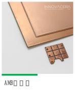
AMB-活性金属ろう付けの紹介
5 Pages
Other Xiamen Innovacera Advanced Materials Co., Ltd products
Metallized Ceramic


Related Searches
- Ceramic
- Insulation ceramic
- Alumina ceramic
- Ceramic plate
- Tubular ceramic
- High-temperature ceramic
- Substrate
- Ceramic ring
- Ceramic rod
- Refractory material
- Zirconia ceramic
- Ceramic substrate
- Wear-resistant ceramic
- Metal powder
- Ceramic disk
- Aluminum nitride substrate
- Protective ceramic
- Ceramic sheet
- Substrate for the electronics industry
- Cylindrical ceramic
*Prices are pre-tax. They exclude delivery charges and customs duties and do not include additional charges for installation or activation options. Prices are indicative only and may vary by country, with changes to the cost of raw materials and exchange rates.